Core platform
TI CC1310
Custom low-power 920 MHz sensor node platform and first complete reference path.
TI CC1352P1
Receiver/reference gateway path for packet reception and human-readable UART decode.
Engineering Notebook · Active R&D
A reusable 920 MHz sensing platform built from custom hardware, measurable event logic and a test-driven low-power architecture.
This independent proof of concept demonstrates how a custom sensor node can detect meaningful local events, preserve environmental context and transmit compact summaries over Sub-GHz RF. It is designed as a reusable starting point for future logistics, food-monitoring and heavy-industrial programmes rather than a fixed single-product design.
Type
Build Log
Status
Functional prototype · Active development
Organisation
Independent engineering R&D
Period
April 2026 to present
Technologies
Methods
At a glance
Role
Product Systems Architect and hands-on development lead
Objective
Build a reusable custom sensor, RF and firmware base for future Industrial IoT proof-of-concept programmes.
Core platform
Custom TI CC1310 sensor node and CC1352P1 receiver.
RF
920 MHz Sub-GHz.
Sensors
LIS2DW12 accelerometer and AHT20 temperature/humidity sensor.
Event processing
Interrupt-driven motion detection with bounded observation windows.
Packet
28-byte versioned observation summary.
Validation
UART, I2C identity, interrupts, spectrum analysis, receiver decoding and Otii power measurement.
Current state
Functional prototype; final deep sleep, enclosure, security and extended field-style testing remain incomplete.
Repository
GitHub source link supplied below.
Source links
Technology stack
TI CC1310
Custom low-power 920 MHz sensor node platform and first complete reference path.
TI CC1352P1
Receiver/reference gateway path for packet reception and human-readable UART decode.
LIS2DW12
Low-power three-axis accelerometer for activity interrupts and motion/event observation.
AHT20
Scheduled temperature and humidity sensing with cached environmental context.
I2C, GPIO interrupt and UART
Sensor bus, activity wake path and bring-up/diagnostic visibility.
920 MHz Sub-GHz
Low-data-rate industrial telemetry where small event summaries matter more than high throughput.
TI EasyLink
RF service foundation for compact observation-summary packet transmission.
28-byte observation-summary packet
Versioned event record carrying motion state, flags, peak acceleration and cached environmental data.
Interrupt-driven wake path
Motion starts local observation rather than requiring continuous host polling.
Bounded observation window
Captures useful state while avoiding raw accelerometer streaming.
Deep sleep planned
Final deep-sleep architecture is still in progress and not claimed as complete.
Code Composer Studio, TI-RTOS and Altium Designer
Firmware build/debug, scheduling and custom schematic/PCB development.
Advantest R3267 and Otii Arc
Spectrum verification and current measurement for scenario-based power modelling.
Logic analysis, Git and GitHub
Digital-interface investigation, milestone control and public source review.
ChatGPT
Architecture discussion, debugging hypotheses, calculations, documentation and prompt scoping.
OpenAI Codex
Bounded repository implementation under explicit instructions and acceptance checks.
Application profiles
Periodic temperature and humidity with movement start/end, shock and drop events for reusable trays, crates or handled loads with sparse movement duty cycles. No customer adoption is claimed.
Temperature, vibration, shock and high-G monitoring, with humidity removal, larger battery and rugged enclosure treated as application decisions. This independent board has not been deployed at a mine.
Reusable drivers, event logic, packet services and receiver tooling that can accelerate future Industrial IoT demonstrators without starting from an empty codebase.
Many Industrial IoT ideas begin with an apparently simple request: measure temperature, detect movement and send the result wirelessly. The difficulty appears later. The sensor has to run from a practical battery, survive a credible environment, report useful events rather than noise, communicate through a defined protocol and provide enough diagnostics to understand failures.
This project was created to establish that foundation before a specific customer programme demanded it. The goal was a reusable Sub-GHz sensing platform that could be adapted to future warehouse, food-logistics or heavy-industrial applications without starting from a blank schematic and empty repository.
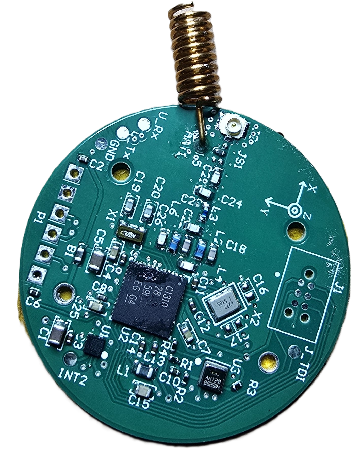
The first complete implementation uses a custom Texas Instruments CC1310 board operating in the 920 MHz ISM band. It combines a low-power accelerometer, temperature and humidity sensing, local event processing and a compact RF packet. A CC1352P1 LaunchPad receives and decodes the packet, creating a working end-to-end path rather than an isolated transmitter demonstration.
Sub-GHz RF is valuable when range, penetration and low node power matter more than high data throughput. The project does not attempt to move large data streams. It is designed to report small pieces of operational information: movement state, shock or high-G events, observation duration, maximum measured acceleration and the latest environmental conditions.
A custom board was essential to the learning and portfolio value. It required decisions about power decoupling, crystal implementation, RF configuration, sensor interfaces, interrupt routing, programming/debug access and physical bring-up. It also exposed the difference between a vendor example and a system that has to work on personally designed hardware.
The board uses an AHT20 temperature and humidity sensor and a LIS2DW12 low-power three-axis accelerometer. The environmental sensor is read on a schedule. The accelerometer provides an activity interrupt to the CC1310, allowing motion to initiate a bounded observation period.
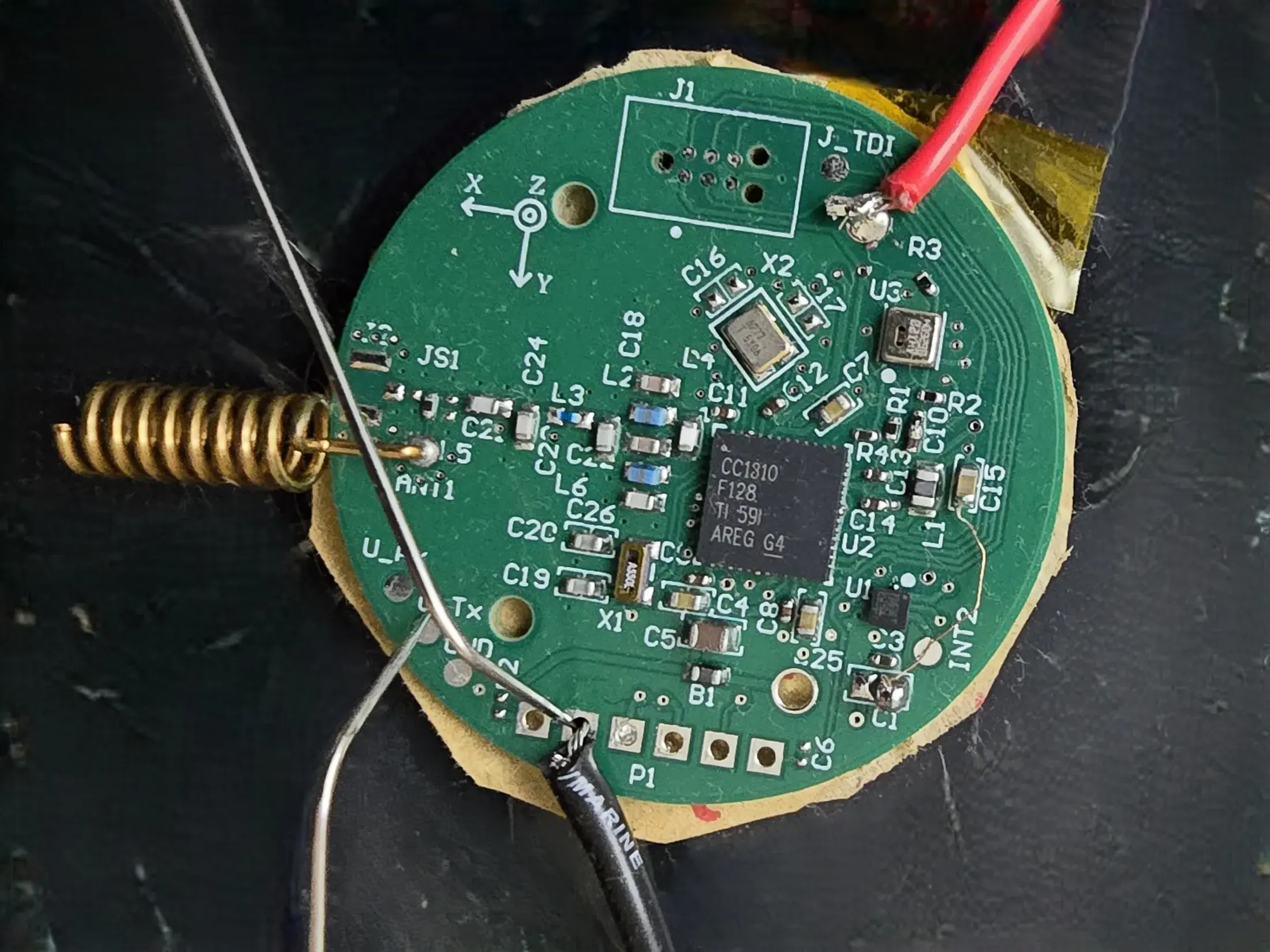
The system starts with a custom CC1310 sensor node. AHT20 environmental sensing and LIS2DW12 motion sensing feed a local observation path. A GPIO activity interrupt flags that movement may be meaningful, after which the firmware performs bounded local observation and event classification.
The node combines the resulting motion state and event flags with cached environmental context and encodes a 28-byte versioned summary. That summary is transmitted over a 920 MHz RF link to a CC1352P1 receiver, which prints a human-readable UART decode.
Future BLE, gateway, MQTT, LTE or cloud paths are roadmap options. They are not presented as completed capability in the current prototype.
A common low-power design mistake is to choose between two extremes: poll continuously or transmit every threshold crossing. Neither produces a good reusable product architecture.
The current platform uses a state-based observation approach. The accelerometer interrupt signals that something meaningful may be happening. The firmware then samples for a bounded period, tracks movement state and maximum acceleration, and sets event flags for conditions such as shock, drop or high-G behaviour. It combines that result with the most recent temperature and humidity values.
The result is not a raw sensor dump. It is a compact observation summary designed to answer practical questions: Did the asset move? For how long? Was there an unusual impact? What was the environmental context? How old is that environmental reading?
The initial RF examples were cleaned of demo behaviour and replaced with a small transmit service and a defined 28-byte message. The message includes protocol identity, version, type, sequence, observation duration, sample count, motion state, flags, maximum acceleration and environmental data.
A CC1352P1 receiver prints the decoded message in human-readable form. This is important because a sensor platform is not complete when radio energy leaves the antenna. The receiving system must identify the packet, interpret the fields and expose enough context to validate the end-to-end behaviour.
The CC1352P1 also leaves a future path toward a demonstration gateway using BLE or a wider bridge. Those features are deliberately kept as roadmap items rather than described as finished functionality.
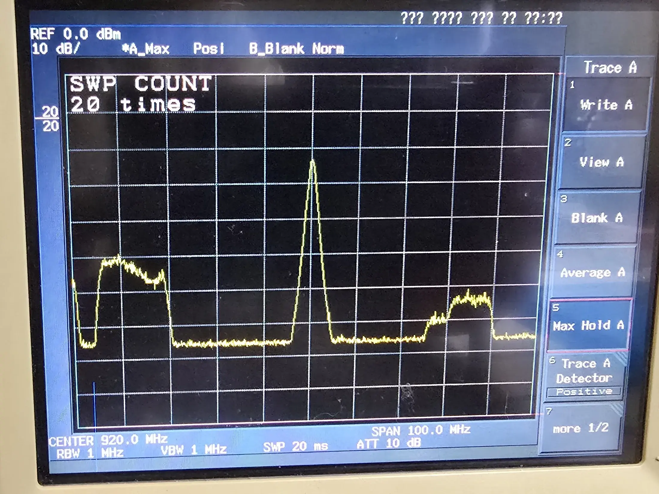
RF transmission was verified as a bench development result, not as regulatory, EMC or certification testing. The important evidence is that the custom node was transmitting at the intended 920 MHz configuration and that the receiver path could turn the packet into readable diagnostic output.
This keeps the validation claim appropriately bounded: the RF path and frequency behaviour were checked on the bench, while range, antenna behaviour after enclosure integration and product-level compliance remain future work.
The current firmware has not yet implemented its final deep-sleep architecture. It still contains development diagnostics, frequent environmental measurement and more rest-state activity than the intended deployment configuration. That makes the present measurements a conservative baseline.
The working model uses approximately 20 µA for the current idle baseline and approximately 2 mA during active observation. With a nominal 620 mAh CR2450, the calculated result depends strongly on how much time the application spends actively observing movement.
Calculated engineering scenarios only. These are not measured field-life guarantees and do not fully include final deep-sleep measurement, battery derating, temperature, self-discharge, RF event energy or real event distribution.
| Active observation | Average current | Nominal calculated life | Interpretation |
|---|---|---|---|
| 20% | 416 µA | Approximately 62 nominal days | Demanding movement scenario |
| 10% | 218 µA | Approximately 119 days / 3.9 months | Regularly handled reusable logistics assets |
| 5% | 119 µA | Approximately 217 days / 7.1 months | Assets stationary for most of their life |
| 2% | 59.6 µA | Approximately 433 days / 14.2 months | Illustrative low-movement case before real-world derating |
A reusable warehouse tray or food container may spend almost all of its time stationary. Temperature and humidity matter; movement start/end and drop events may be more valuable than frequent motion packets. A small coin cell can be appropriate if the RF and observation policy remains sparse.
A mining or heavy-industrial sensor has a different profile. Humidity may provide little value and can be disabled. Temperature, vibration, shock and high-G behaviour may dominate. The enclosure and battery can be larger, and thresholds need to reflect the machine rather than a handled tray.
The project therefore separates the platform from the product configuration. The CC1310 board, drivers, event logic and packet services provide a reusable base. Sensor selection, battery, enclosure, thresholds and reporting intervals remain programme-level decisions.
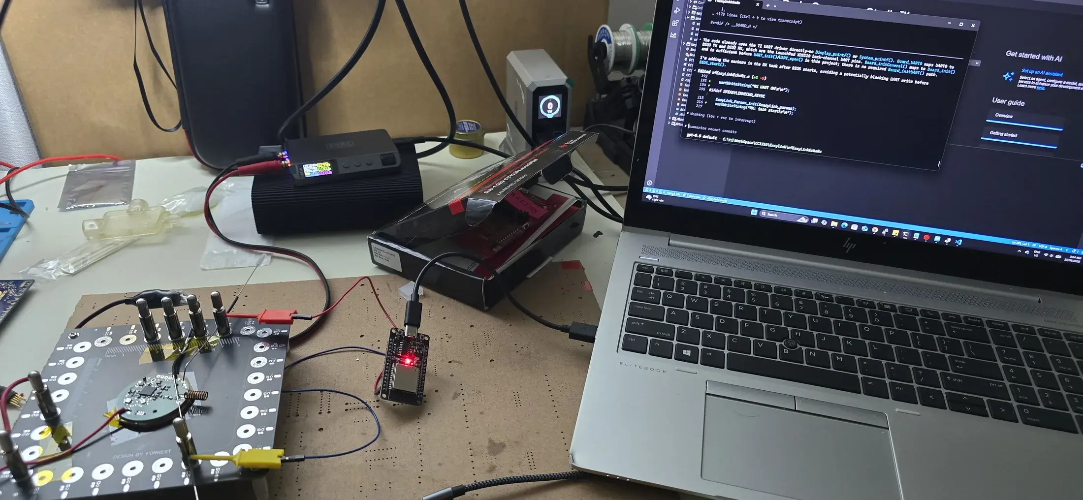
The project was supported by more than a development board and serial terminal. RF output was checked on an Advantest R3267 spectrum analyser. Current behaviour was examined with an Otii Arc. Digital interfaces and UART paths were investigated using logic-analysis tools.
XDS110 debug and application UART supported flashing, break/debug work and serial diagnostics. CC1310 and CC1352P1 LaunchPads supported reference hardware, receiver development and comparative bring-up. Rework and inspection tools supported custom-board assembly correction and bench work.
The wider bench includes oscilloscope, RF-network, component-measurement, programmable-load, fine-rework and macro-photography capability. The engineering message is that the design loop was closed through physical measurement rather than compilation or simulation alone.
This project was developed in 2026 with deliberate use of generative AI. ChatGPT supported architecture discussion, debugging hypotheses, test planning, calculations, documentation and bounded prompt creation. Codex performed scoped repository implementation under explicit instructions.
The human responsibility boundary remained clear. Raghav defined the objective and architecture, designed the custom hardware, built and flashed firmware, operated instruments, interpreted evidence and accepted or rejected changes.
Generated changes were validated using builds, UART logs, spectrum analysis, RF reception and current measurements. The current product does not contain AI or machine learning; AI was part of the engineering workflow, not the device function.
The project includes useful failures and design turns. Early I2C behaviour included timing and data-readiness issues. The receiver initially had UART visibility problems, which reinforced that a radio demo without observable receive-side evidence is not an end-to-end system test.
Vendor demo RF behaviour was removed rather than allowed to become the product architecture. The initial transmit-after-observation approach also exposed a communication-policy gap for long-lived motion, shifting the design direction toward movement start/end, significant event reporting and optional bounded heartbeats.
Active observation dominates the high-movement power scenario, so environmental interval tuning alone is not enough. Deep sleep, enclosure, security, provisioning, multi-device behaviour, regulatory work and production hardening remain incomplete.
The platform is a functional development prototype and active proof of concept. Completed work includes custom CC1310 PCB bring-up, UART, AHT20, LIS2DW12, interrupt path, bounded observation, the 28-byte summary packet, 920 MHz transmission, CC1352P1 reception and decode, early power modelling and Git milestones.
In-progress work includes the deep-sleep state manager, event-only reporting policy, configurable environmental interval, 14 dBm versus 10 dBm comparison and representative duty-cycle measurements.
Planned work includes a 3D-printed enclosure, range and endurance testing, antenna review after enclosure integration, security and provisioning, a polished end-to-end demonstrator, and future Nordic Semiconductor and Silicon Labs reference work. These roadmap items are not presented as implemented.